
In anticipation of the Space on @oxidecomputer lab tales this afternoon, I figured we'd give a peak behind the curtain of power delivery validation for one of the large ASICs in our system. So.. a short 🧵. Note this work is primarily @random_enginerd, I am just the narrator :)
High-end ASICs such as networking switches, GPUs, etc., manufactured on small process nodes require a relatively low voltage for their transistors to switch (0.7V-1.2V) but their sheer number and often high clock frequency requires heaps of current (in the order of 100s of Amps).
While an ASIC is powered up, its power rails need to stay within a relatively narrow acceptable range; if the voltage is to high you risk damaging the device, if it is too low transistors may not switch reliably, causing bit errors, unexpected behavior and/or damage.
When an ASIC suddenly needs to perform more work it may draw a proportional amount of additional current (as a result of the transistors switching), referred to as a load step.
Because the power delivery network (PDN) implemented on the circuit board can't provide this current instantaneously, the voltage level of the power rail will droop (hand-waving over why this happens), potentially below that narrow acceptable operating range.
A similar effect occurs when a large portion of the device suddenly stops switching, causing an excess in current, and the voltage suddenly going up (because the PDN is still supplying more current than needed), potentially exceeding the limits and damaging the device.
Finally, virtually all of the power we pump in these ASICs results in heat which needs to be dissipated. W = V^2/R dictates that a higher voltage of the power rail will result in more heat.
R is intrinsic to the device, so the only knob available to reduce heat is trying to keep the voltage as low as possible. Or rather, keep that voltage range as narrow as possible while keeping the ASIC within operating conditions for all possible conditions/configurations.
The ASIC design/validation process establishes the PDN operating parameters, resulting in system requirements such as; given a base load of X amps, allow for a load step/release of Y amps in Z us (or even ns), while keeping the voltage within +/- some amount of mV.
Armed with these requirements, PDN components are selected and a first round of calculations is done to determine if the control loop can meet the required load step/release. This is primarily done using spreadsheet tools and design input provided by manufacturers.
Next up is doing early PCB layout (which can only negatively impact your perfect first order calculations), and import the resulting board geometry into a simulation tool to do a detailed PDN analysis. This ultimately results in graphs like this:
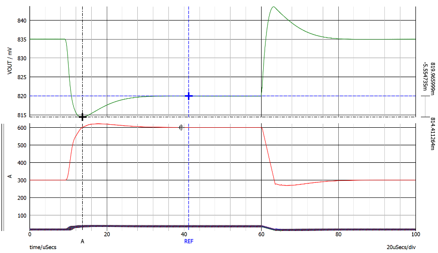

These simulations involve fairly detailed models from the PDN component suppliers (including controller tuning parameters), to get as accurate a prediction of system performance ahead of building the actual board. But ultimately you will want to validate on an actual board.
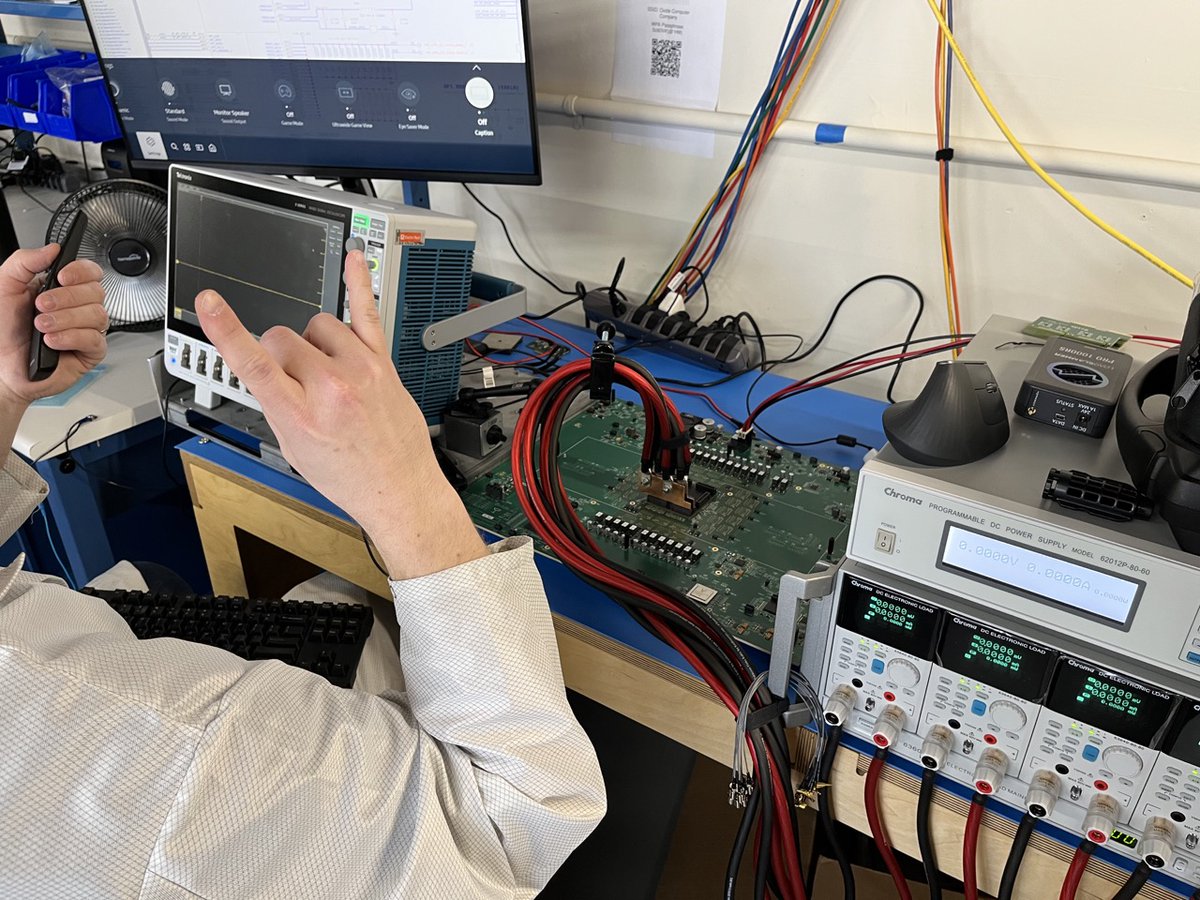
Testing/tuning using a synthetic workload produced by the ASIC itself is a cumbersome process, where you may not be able to control the test parameters you care about. Instead we opted to use a solution from LoadSlammer ().
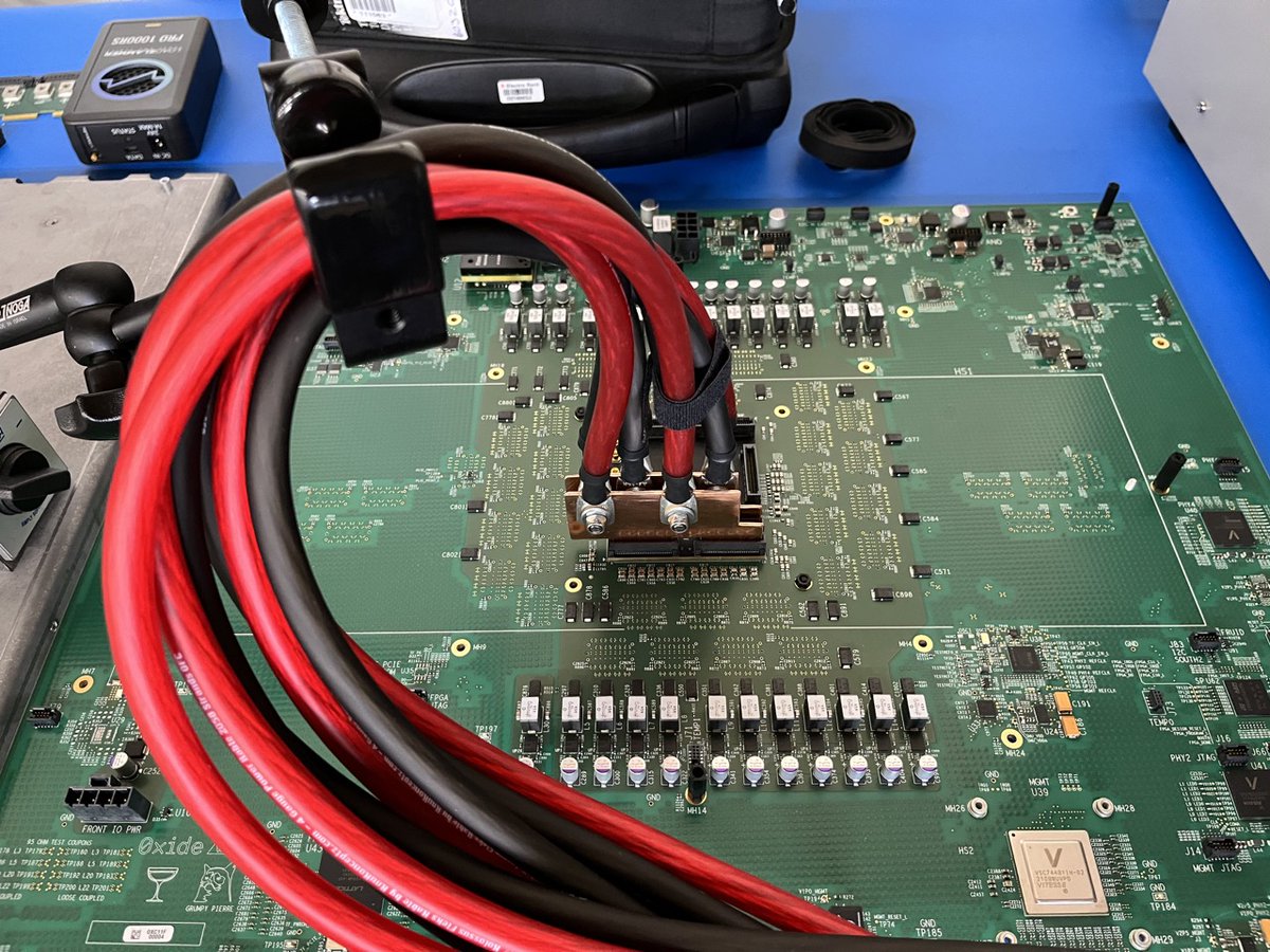
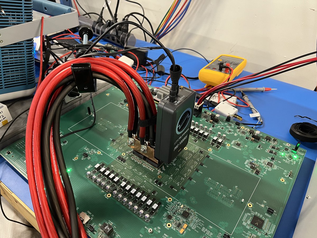
This uses a custom BGA adapter, matching the ASIC pinout and closely emulating the PDN properties of the real system.

The BGA adapter is shown in the center of the board, connected using thick copper cables to a programmable static load. This load is configured to apply a several hundred amps base load, simulating the ASIC in steady state.
A LoadSlammer is then added, which lets us generate a controlled load step/release with parameters of our choosing (by effectively causing a controlled short between + and -). This simulates the ASIC suddenly drawing more or less power.
The software provided with these LoadSlammers lets you run many experiments in a short amount of time, providing a statistical basis for analysis results and letting you tune PDN parameters in minutes/hours rather than days.
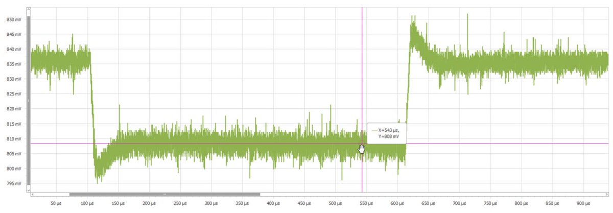
Positive correlation between the results generated using the LoadSlammer and the earlier simulations provide confidence that the design and configuration meets the ASIC power requirements.
But equally important to us; it lets us tune the narrow voltage window in which we need to operate the PDN such that the nominal voltage is as low as possible, reducing the heat generated by the ASIC.
Do join the Space this afternoon for more bring-up stories or catch the recording (will post a link once available) as we'll probably dig into this setup some more.
The cables are only used to connect the static base load. They do physically move when we initially turn on the 300A load, but there are no significant transients after that.