
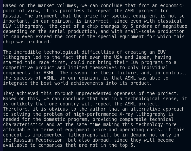
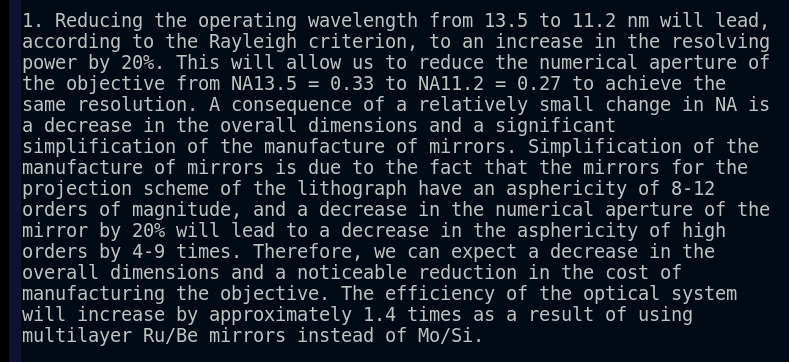
🧵 Russia's X-Ray Lithography Program. I have a preprint of the paper by Nikolai Chkhalo, of the Institute of Physics of Microstructures of the Russian Academy of Sciences (IPM RAS). It's an impressive piece of work! Pros: It does a very good job addressing the economic aspects
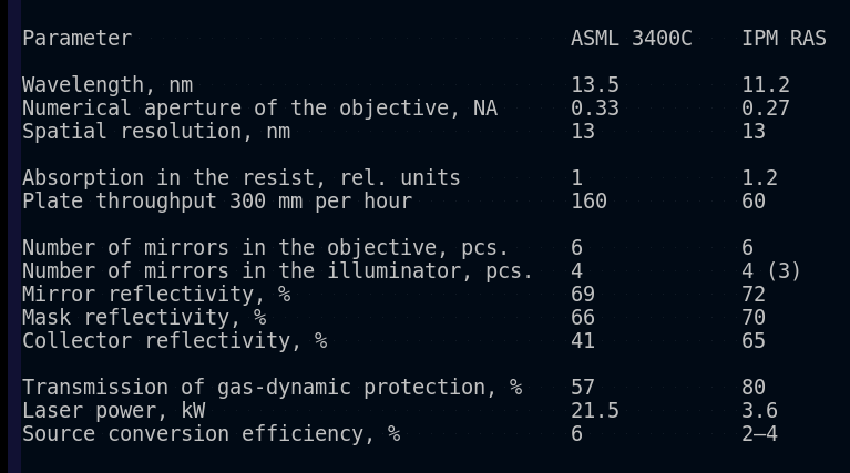
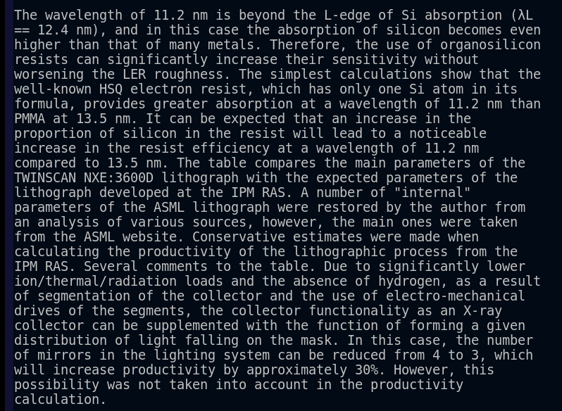
Here's a translation of the comparison table to ASML's tool. The overall concept for the new tool is to match the resolution to ASML's EUV scanner at a much lower cost—both for the tool itself and the operational costs. It's much slower, but this is offset by the reduced costs,
Sources: A preprint of the paper can be downloaded here: https://disk.yandex.ru/i/STNu0... There will be a full version published in the journal of Microelectronics. 12/5 - An article by Nikolai Chkhalo, the author, summarizing the preprint called "A chance for a Russian lithographer"
The core argument here for a radically different approach is that ASML's EUV scanner is cost prohibitive to all but the top 5: TSMC, Intel, Samsung, Micron, and SK Hynix (you could throw Rapidus and SMIC in the mix here as well). So regardless of what the throughput is, the tool
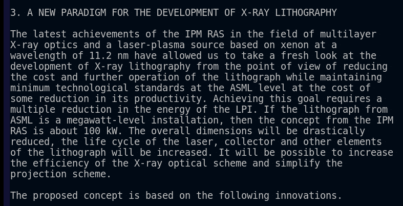
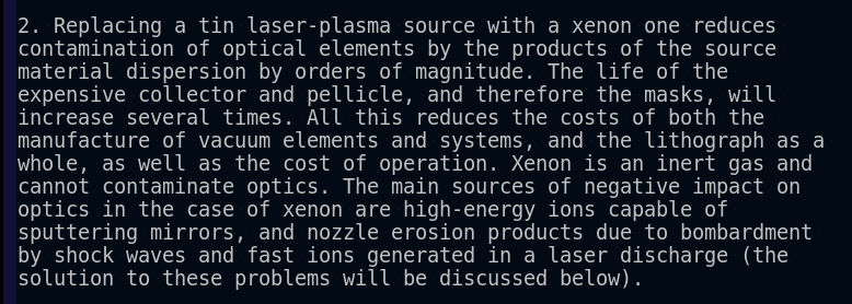
They've developed a laser-plasma source based on xenon and the new multi-layer mirrors to go with it; it operates at a wavelength of 11.2 nm. There are 3 reasons they think this will be more cost effective…
Remember, the core mission is to match the resolution of ASML's EUV scanner. And they don't even need to do that, which allows them even more wiggle room on reducing the costs. They are able to relax the NA of the lens quite a bit, and this makes for a smaller, simpler lens
Operational costs are reduced with what they are claiming is a cleaner source system. Conventional tin-plasma is dirty, contaminates the optics, and reduces lens transmission. A massive amount of hydrogen gas is needed to keep everything clean. If they are right, this potentially
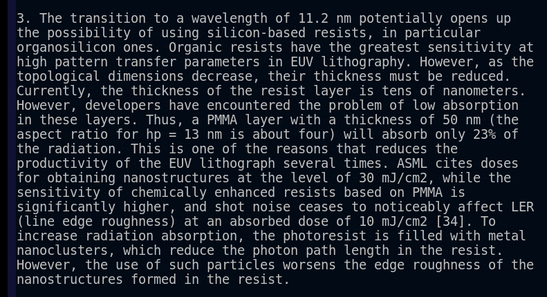
Silicon Photoresists: They are claiming that silicon resists at 11.2 nm would have even higher efficiency than the metal oxide resists in development today. This potentially gets around the shot noise issue and ultimately the productivity issue as well. And guess what, there was
@lithos_graphein Is this real? The word for preprint is just preprint using cyrillic letters?
@MadHermitHimbo Real.
@lithos_graphein Maybe they mention how they overcome the large increase of stochastic noise?
@JamesDSneed They essentially try to match it to ASML's low-NA tool.
@lithos_graphein It does not yet say anything about the other machines in the lithography supply chain, such as overlay tools, ADI and AEI, depostion and coating tools for this type of photoresist and the software tools. Perhaps they will show them in the future or get them from China.
@throwaway3313 Some of those were part of their semi plan released earlier in the year. although it was very low funding
@lithos_graphein Overlay concern comes from reliance on LELELELE... type multipatterning.
@DrFrederickChen They're just skipping immersion entirely. As a concept it's not bad.
@lithos_graphein How did you even end up with finding that work? :) Interesting read, indeed, always curious what our scientists consider to be feasible in... well... overall situation.
@pastaraspberry its all public online
@lithos_graphein Do you have the research paper this topic is interesting
@aq_lp0 here it is: https://disk.yandex.ru/i/STNu0...
@lithos_graphein Iirc for atleast a MIL standpoint, mass production is fine for 22nm. They high end new nodes only need few units since advanced wep production isnt in mass production fully yet. Just what i heard 🤷♂️
@lithos_graphein https://x.com/TroyJamesMonger/... As I understand it, the overlay issue is the result of using relatively coarse ArF immersion lithography (193 nm). Considering x-rays are 0.1 - 10nm in wavelength, compared to EUV's ~13.5nm, I guess I don't see why there would be anymore alignment issues