
[1/16] 🧵 A History of ASML’s Scanners Enabling the AI Revolution with chip printers—the most complex machines ever built.


[2/16] The List Here we have my list of all the ASML’s scanner models installed over the past 35 years. It’s not an exhaustive list; I’m sure I’ve missed a few, but it’s what I was able to put together based on the tools I’ve run (which is most of them) or models my friends have

[3/16] Scanner Platforms When we think of the different generations of lithography tools that have been developed over the years, we often associate each generation with the light source. Generally speaking, the smaller the wavelength of the source, the smaller the circuit

[4/16] Scanner Platforms Continued… ASML has developed 5 scanner platforms over the years, and each platform had a series of tool models released where iterative improvements were made to both the overlay and throughput such that fabs could get improved ROI on their lithography

[5/16] TWINSCAN XT Platform: This was the first dual-wafer stage platform. There were other major changes to how the optics were configured, but the addition of an extra stage is what really affected the ROI. To fully appreciate how big a change it was, it should be noted that

[6/16] Pattern Alignment and Overlay: These are often used interchangeably, but in litho world, these are very different things. Alignment is what the scanner does to place a chip image on top of another one. Overlay is simply a measurement of the placement error after the fact,

[7/16] TWINSCAN NXT Platform: The NXT platform made a big change to how the wafer stages fundamentally work. The prior stage generations relied on the stages to be suspended over a flat backplane using air pressure. It floats in a frictionless way and can move independently

[8/16] Overlay vs. Stage Speed—A Modern Marvel ASML’s scanners have a throughput of roughly 200-300 wafers per hour depending on the model. For the latest KrF scanners being developed, ASML intends to push this even further to 400 wph. - At 250 wph, this equates to a full wafer
[9/16] Immersion Lithography I feel obliged to briefly explain another feat of engineering that will play into my final points at the end of this thread. The latest logic and memory chips heavily rely on a new type of scanner technology called immersion lithography. In short, the
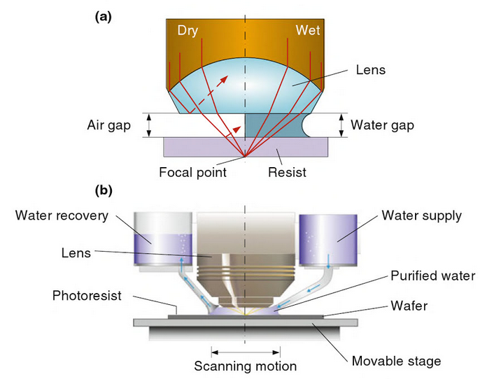
[10/16] The EUV Era We’ve discussed the DUV platforms and what ASML was working on for 35 years to improve their commercial viability. But as we jump into the two EUV platforms, we have a new set of engineering challenges that make that development work seem simple. Whereas the

[11/16] The EUV Development Timeline EUV lithography is the most complex and ambitious undertaking in lithography to date. It's arguably the most complex machine ever made on a commercial scale. The development for it started back in the mid-1980s and continues to this day. ASML

[12/16] Exposing Product Wafers Drives Learning Let’s revisit our list of ASML’s scanner models again; refer to Column C for the tool types. As you can see, the vast majority of these tool models were HVM machines running product wafers in the fabs that today can cost as much as

[13/16] Lithography is Winner Take All. The graveyard of scanner companies is full. One might think this is due to how other companies fail in their line of business—a botched product launch, missed timelines, economies of scale. Here again lithography is a different beast. The

[14/16] The Chip War Advanced lithography tools are at the heart of the chip war. Indeed, the first salvo fired over the bow was the banning of ASML’s EUV scanners from export to China. This was followed by 2 export actions blocking the most advanced DUV immersion systems made by

[15/16] So how long then? 2035 NXT:2000i equivalent specs 2045 NXE:3800E equivalent specs - Look at this list and tell me it won’t take at least 20 iterations and a fleet of new models being installed every year? - How many wafers need to be run on each new model? - How do you

[16/16] Overlay = 3 meters [end]
@lithos_graphein We have quite cool educational trainings about our products and roadmaps at Zeiss, too🔥🥰
@b4ud3r Do a thread on X! 🍻
@lithos_graphein ASML had to pathfind, nobody did it before. China will have all blueprints and key personnel from ASML & all suppliers. And I'd bet there are more Chinese nationals in graduate engineering programs in the USA + maybe EU than locals citizens. Then add China's own universities.
@lithos_graphein Your thread is going viral! #TopUnroll https://threadreaderapp.com/th... 🙏🏼@rwang07 for 🥇unroll
@lithos_graphein @threadreaderapp unroll
@lithos_graphein @threadreaderapp unroll please
@lithos_graphein Thanks, terrific Thread